
Microelectronics is arguably the most critical example of advanced manufacturing, representing a $442B/year global economic engine that is essential to the U.S. economy and its physical and energy security. Improving microelectronics manufacturing to atomic scale precision is critical to realizing technologies such as quantum and spin-based devices that will enable transformative compute capabilities while reducing carbon emissions. Achieving this promise requires patterning control well beyond current methods and materials.

We seek materials and processes that:
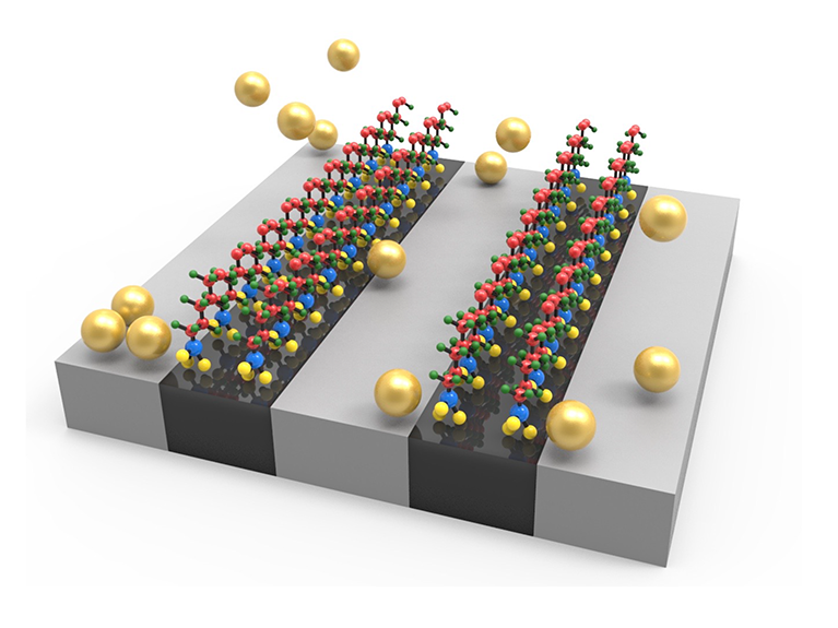
- Efficiently harness high energy photons to perform selective chemical reactions that can be leveraged for atomically-precise patterning at the nanoscale
- Mitigate stochastic effects, i.e., the variability that arises from photon, atom and molecular scale variations that ultimately limit sub-nm level precision
We are developing knowledge of radiation-driven reactions at EUV photon energies in order to design new materials that are highly sensitive, highly uniform in chemical response, and with controllable interfacial interactions. We are using hierarchical materials under kinetic control to mitigate the stochastics from imaging and to provide functional sites for area-selective pattern transfer.

Progress has been hindered due to:
- Lack of a fundamental understanding of EUV-radiation-driven chemical reactions
- Poorly controlled diffusion in reaction fronts with heterogeneous photoresists
- Lack of understanding of solvation at nanointerfaces when developing the images
- Lack of design rules to build self-assembling systems that at once satisfy the thermodynamic, kinetic and functional properties to perform as lithographic materials below 10 nm.
- Insufficient understanding of the chemical physics of atom-addition/removal during area-selective deposition or etching.

Addressing listed gaps will impact far more than just patterning science. Understanding of low-energy electron chemical pathways could lead to new routes for chemical transformations and synthesis; breakthrough tools for studying solid–liquid–gas interfaces could deepen our understanding of electro-chemo-mechanical phenomena in energy systems; and guiding kinetic trajectories in multi-component self-assembly could enable novel properties from complex materials hierarchies.
We support workforce development in microelectronics manufacturing. CHiPPS is sponsoring four training stipends per year for San José State University undergraduate or master students in STEM fields. The training program hosts students for ten weeks at Berkeley Lab or Stanford and teaches critical skills relevant to patterning science for lithography and nanopatterning.