
Michael Tsapatsis, Johns Hopkins University
10-11am, March 24, 2026 Zoom
Amorphous Zeolitic Imidazolate Frameworks (aZIF) as Resists for EUV and BEUV Lithography
Advancements in lithography have focused on shorter exposure wavelengths and new resist types to enable finer feature patterning, resulting in denser integrated circuits and more efficient chips. However, current resist technologies may not meet future demands outlined in technology roadmaps for sub-nanometer nodes, which target features down to 5 nm and below. We introduced a class of amorphous metal organic frameworks (amorphous zeolitic imidazolate frameworks: aZIFs) as resists for electron-beam lithography (EBL), extreme ultraviolet lithography (EUVL: 13.5 nm), as well as for lithography using smaller wavelengths, beyond EUV (BEUV: 6.7 nm). The sensitivity and tone (negative or positive) of aZIFs can be tuned by the choice of metal and imidazole, and by the selection of appropriate vapor or liquid development methods. aZIF resists can be deposited by ALD/MLD, as well as by spin-on methods, with excellent control of compositions, thickness, and wafer-scale uniformity.
In this talk, I will give a historical perspective of ZIFs starting from Professor Yaghi’s group discoveries that established this class of materials, describe their solvothermal and vapor phase synthesis, their solubility in aqueous solvents, and their sensitivity to low energy electrons, which led us to propose them as lithographic materials (Angew. Chem. Int. Ed. 57, 13592-13597 (2018)). The current status of development of aZIF resists will then be described based on our recently published work (Chemistry of Materials 37(21), 8548–8567 (2025), Nature Chemical Engineering 2, 594-607 (2025)), followed by a description of our ongoing efforts to exploit the rich compositional space of a ZIFs to improve their sensitivity and resolution.
Alex Robinson

August 26, 2025
The Multi-Trigger Resist
Emily Gallagher

July 22, 2025
Climate-aware IC Manufacturing
Gila Stein

May 27, 2025
Catalyst Diffusion in Chemically Amplified Resists
Cheng-Hao (Will) Wu

March 25, 2025
Dry deposition and dry development of metal oxide resist and its extendibility to high NA EUV lithography
Douglas Guerrero

Jan 28, 2025
A more sustainable method to disrupt traditional wafer processing in lithography
John Petersen

Dec 4, 2024
Probing Extreme Ultraviolet Exposure of Photoresists
Grant Wilson

September 25, 2024
Materials for High Resolution Imaging Applications
Greg Parsons

August 28, 2024
Inhibitor-Free Area-Selective Deposition via Combined Atomic Layer Deposition and Etching
Daniel Sunday

June 26, 2024
Depth Profiling Structure and Orientation in Confined Soft Matter
Roberto Fallica
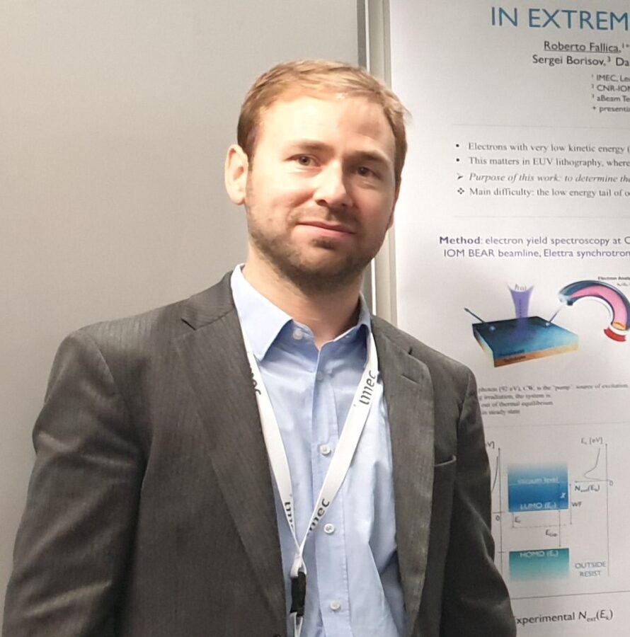
May 22, 2024
Characterization of EUV materials: from well-established to pioneering methods
Patrick Naulleau

April 24, 2024
Benefits and challenges of phase shift mask technologies in the EUV regime
Lander Verstraete

March 27, 2024
Directed Self-Assembly: a Perspective on Line/Space and Contact Hole Patterning for Logic and Memory Applications
Sonia Castellanos

January 24, 2024
The soft side of metal-oxide resists