
The mission of the Center for High Precision Patterning Science (CHiPPS) is to create fundamental understanding and control of patterning materials and processes for energy-efficient, large-area patterning with atomic precision, thereby enabling at-scale advanced manufacturing of future-generation microelectronics such as quantum computing and spin-based memory and logic devices.
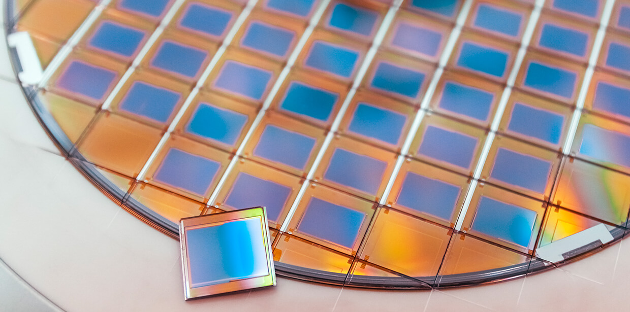
CHiPPS is employing a holistic approach to patterning science that incorporates knowledge of radiation-driven reactions at extreme ultraviolet (EUV) photon energies to design new materials that are highly sensitive, highly uniform in structure and chemical response, and with controllable interfacial interactions during pattern development.
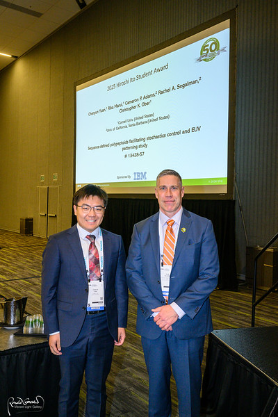
Chenyun Yuan wins the Hiroshi Ito Student Award award for best student paper at SPIE
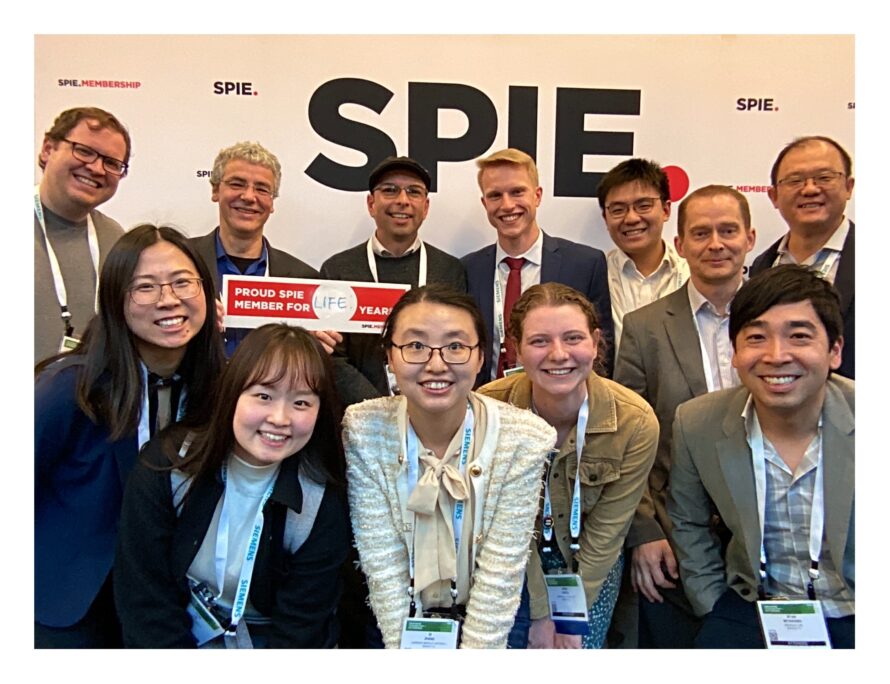
CHiPPS at SPIE Advanced Lithography & Patterning
JVSTB paper highlighted in AVS newsletter

Recent Publications
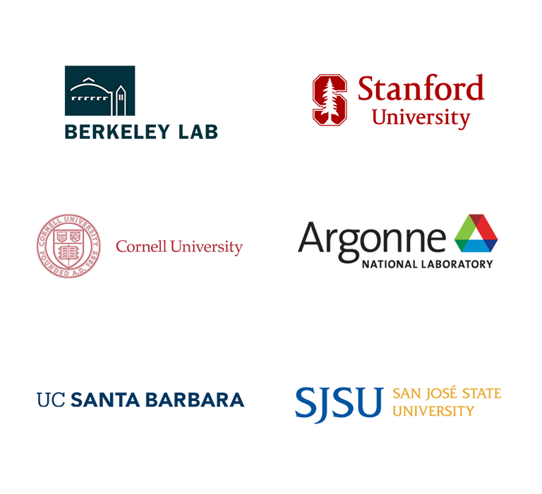
As an Energy Frontier Research Center (EFRC) funded by the U.S. Department of Energy, CHiPPS is led by Berkeley Lab and is a large collaborative effort of scientists at six participating institutions.